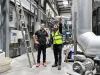
As the company boasts some of the most advanced equipment in the industry, CCO Peter Dijkstra discusses how Trymax Semiconductor Equipment B.V. has achieved this unique position.
WHEN PLASMA MATTERS
Amongst many titans of the manufacturing industry in the Netherlands, Trymax Semiconductor Equipment B.V. (Trymax) is the company of choice for the design, manufacture and marketing of plasma-based processing and equipment solutions.
Trymax was first founded in 2003. Its name stands as a re-lettering of the Matrix plasma asher machines that are widely regarded in the industry.
“Our mission was clear, to provide service and support for European customers who depended on Matrix-like machines,” Peter Dijkstra, CCO of Trymax begins.
As time went on, the company faced new challenges; between 2007 and 2009, it realised that the ageing Matrix machines had exceeded their serviceability limits, prompting Trymax to start manufacturing its own equipment.
This signified a major transformation, as it shifted from a service-orientated provider to a cutting-edge manufacturer.
“This strategic move allowed the organisation to adapt to the evolving semiconductor landscape and stay at the forefront of technological advancements,” Dijkstra tells us.
PRECISION PERFORMANCE
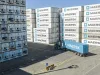
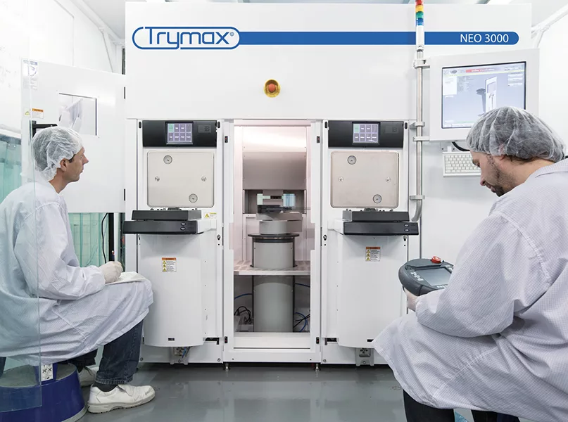
Trymax’s headquarters, situated in Nijmegen, has an impressive total capacity of 4,200 square metres (m2), which includes a manufacturing cleanroom, a state of the art demo lab, an engineering and manufacturing area, and a logistics, storage, and technical area, with an equipment build capacity of up to 250 toolsets per year.
When situated within the wider network of facilities, Trymax is proud to be the number one European semiconductor equipment cluster, with one of the strongest supply chains. This position is bolstered by the fact that Trymax does all its final assembly and testing in-house, ensuring streamlined operations and maximum efficiency across its entire production.
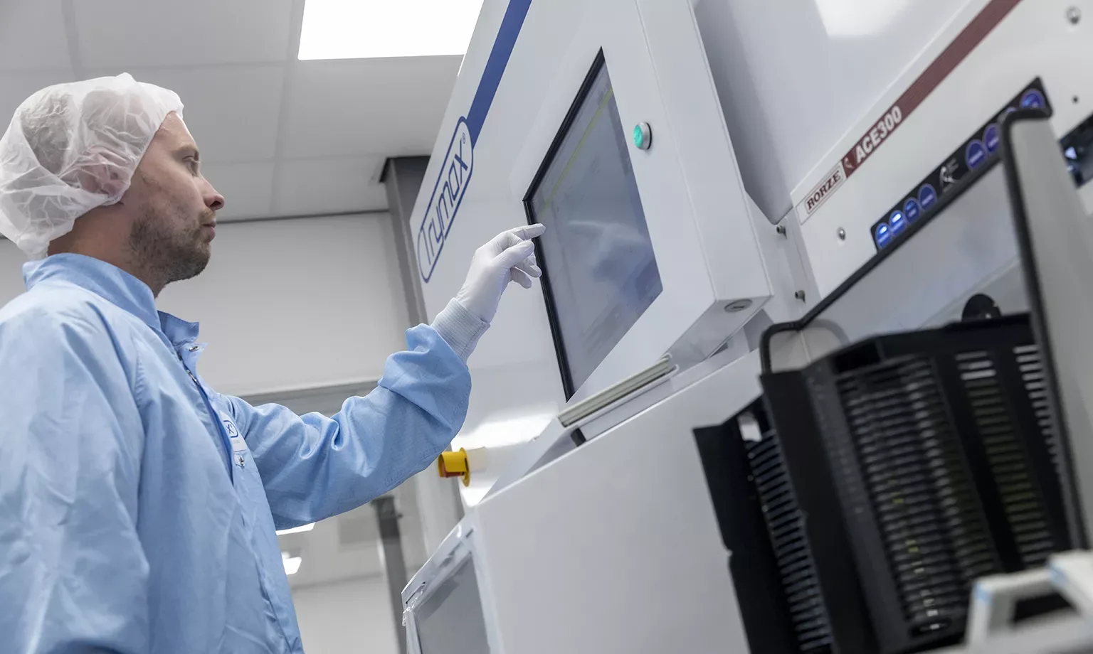
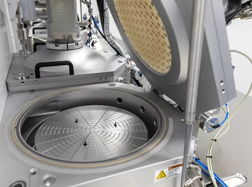
The company’s service offering entails diligent plasma solutions in ashing, descumming, etching, surface preparation, and ultraviolet (UV) curing and charge erasure. To achieve this, Trymax provides an industry-leading product line known as NEO, which is designed to address a wide range of applications throughout the semiconductor manufacturing process.
All platforms found in each NEO can handle two or more substrate types and sizes simultaneously without any hardware changes. Furthermore, each product has a strong focus on all types of substrate handling, catering to substrate sizes from 77 millimetres (mm) up to 330mm, with a focus on 150mm, 200mm and 300mm. Further features include platform flexibility with five different process modules, alongside a detailed system configuration based on the application specification budget.
With a global network of processing chambers, Trymax puts its burgeoning success down to the precision of its NEO products, as its equipment sets the company apart with its ability to process two different wafer sizes simultaneously. This feature proves particularly valuable in a transitioning market, such as the LED industry, in which Trymax’s machines can process wafer sizes from 150mm to 200mm, outrunning older machines that need extensive modifications to accommodate new wafer diameters.
“By already accommodating varying wafer sizes, Trymax’s machines mitigate the risks associated with equipment reconfiguration,” elaborates Dijkstra.
“An additional feature is the machine’s automatic recognition of wafer size and the ability to handle it seamlessly, streamlining production processes and enhancing efficiency.”
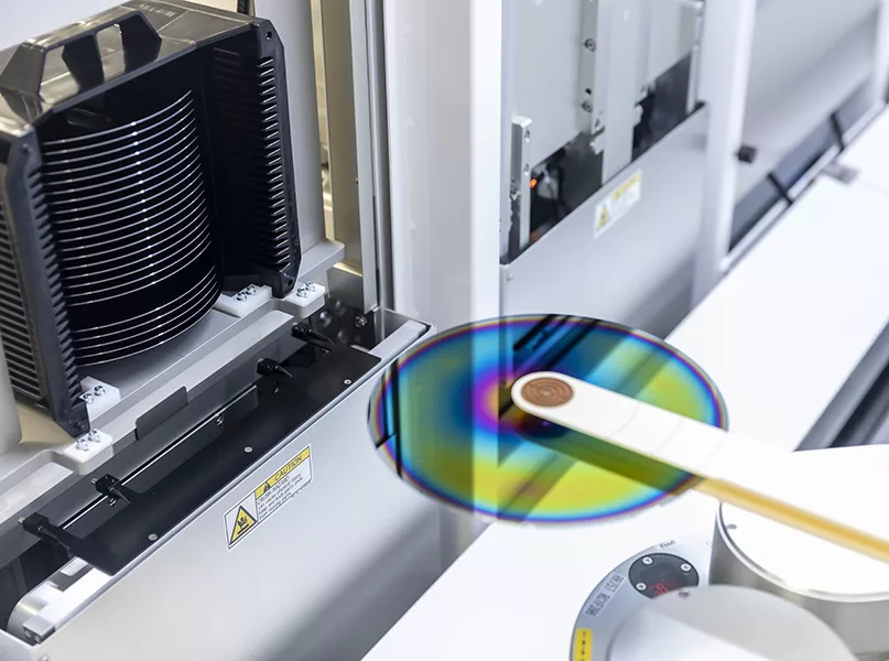
At the peak of Trymax’s innovative solutions, it deploys a sophisticated robot arm that can be equipped with several specialised substrate gripping tools, designed for a diverse range of uses, whilst greatly advancing the organisation’s product line.
CONTRIBUTING TO A BETTER WORLD
Correlating with the technical innovations of the company, Trymax is honoured to participate in a multitude of projects that facilitate a better and more sustainable future. Projects like SMART Photonics, for example, allow a much higher data exchange rate by using optical communication. This offers a vital aid to hospitals, providing significantly important components to a vast range of medical equipment.
Additionally, the power management integrated circuits (power IC) markets in each NEO have recently had a renewal, as the silicon was replaced by short interval control (SiC) material.
“Industry leaders have made a calculation that suggests if we replace all silicon material for power applications by SiC, we can skip 880 nuclear power plants worldwide, making a huge impact,” Dijkstra informs us.
Furthermore, as a key support to the company, Trymax’s logistics supply chain is essential for streamlined operations. Receiving all components and materials on time results in shorter lead times.
“We work very closely with all our suppliers. A good example of this was during the COVID-19 pandemic when a major German customer ordered several ashing tools. We couldn’t supply all the tools on time, due to missing an essential component from a German company.
“Following our customer’s intervention, who purchased the missing component, we managed to reduce the delayed shipping time, providing an indispensable helping hand,” he recalls.
QUALITY AND QUANTITY
As the year continues, Trymax is focusing on increasing its market share in the manufacturing industry. It has much to look forward to as the semiconductor sector expands its capabilities, including new UV curing technology.
To be a proactive part of the industry shift, the company brings to the fore the NEO 2000UV tool, an advanced UV curing and charge erasure system which utilises a single UV bulb. The new equipment acts as a bridge tool for two wafer diameters and is specifically designed for applications from three to eight-inch substrates, enabling greater accuracy.
Consequently, due to its highly ultra-modern technology and influential presence in the industry, Trymax has experienced market recognition from many major automotive suppliers to the German, South Korean, North American, and Japanese car industries.
“We’re currently number one in Europe and number two in China. Additionally, we recently opened a sales and service office in the US. As such, our target is to increase sales, but without losing quality, performance and innovation,”
Dijkstra closes.
TRYMAX SEMICONDUCTOR EQUIPMENT B.V. PARTNER